Circuit boards are the foundation of modern electronics. Every button you press, sensor you trigger, or display you read is connected to a printed circuit board (PCB) doing the work behind the scenes. Building these boards at scale is no small task. It takes precise processes, strong quality control, and the proper infrastructure to do it consistently. This is what separates professional circuit board manufacturing companies from the rest.
Let’s take a look inside how these companies work and what they do to keep production on track from day one.
Step 1: Reviewing the Design
Before production begins, manufacturers review the design files. These usually include Gerber files, netlists, BOMs (Bill of Materials), and sometimes 3D mechanical drawings. This early review helps spot errors before they hit the production floor.
For example, engineers might catch:
- Missing solder mask openings
- Drill holes too close to board edges
- Components that won’t fit the footprint
- Trace widths that can’t support the required current
Most experienced circuit board manufacturing companies run what’s called a DFM (Design for Manufacturability) check. This step prevents costly redesigns or rejected batches down the line.
Step 2: Material Selection and Stackup
Once the design is cleared, the manufacturer selects materials. Different applications require different types of substrate, copper thickness, and solder-mask color. Boards that go into industrial or medical devices may need special coatings or heat-resistant layers.
The “stackup” refers to how these layers are arranged. A 6-layer board, for example, might have power and ground planes in the center with signal layers on the outside.
Getting this structure right is key to:
- Signal integrity
- Thermal performance
- Overall board strength
This step is especially important for high-speed or high-power applications.
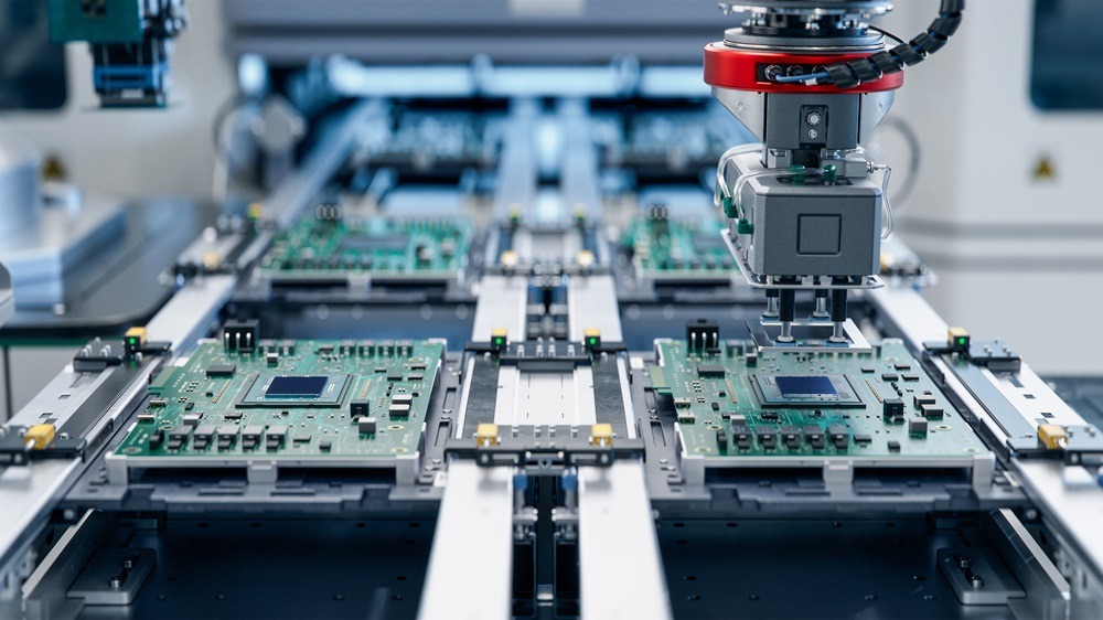
Step 3: Imaging, Etching, and Drilling
This is where the manufacturing really starts.
- Imaging: The copper-clad board is coated with a light-sensitive film. The PCB layout is then printed onto it using UV light.
- Etching: The unwanted copper is removed, leaving behind the traces and pads.
- Drilling: Holes for vias and through-hole components are drilled, sometimes down to micro-scale precision.
In advanced facilities, laser drills are used for tiny holes in HDI (High Density Interconnect) boards.
Step 4: Plating and Solder Mask
Once drilled, the holes are plated with copper to connect different layers of the board. Then, a solder mask is applied. This is the colored coating (often green) that protects the copper and prevents solder bridges during component assembly.
This step might seem simple, but poor plating or uneven solder mask can cause shorts, corrosion, or weak solder joints, which can lead to field failures.
Step 5: Silkscreen and Surface Finish
Next comes the silkscreen layer. This includes component labels, test points, and other text that helps during assembly and troubleshooting.
Then a surface finish is applied to the exposed pads to protect them and prepare them for soldering. Options include:
- HASL (Hot Air Solder Leveling)
- ENIG (Electroless Nickel Immersion Gold)
- OSP (Organic Solderability Preservatives)
Each one has different trade-offs in cost, shelf life, and performance.
Step 6: Quality Control and Testing
This is where circuit board manufacturing shows its discipline. Every board is inspected, often using a mix of:
- AOI (Automated Optical Inspection) for visual defects
- X-ray inspection for multilayer board analysis
- Electrical testing to check for open circuits and shorts
Some circuit board manufacturing companies also offer flying probe tests or in-circuit testing, depending on the project needs.
Failures at this stage are rare in well-run facilities. But when they do happen, manufacturers trace the problem back to the exact step and correct it before more units are affected.
Step 7: Packaging and Shipment
Finished boards are cleaned, baked to remove moisture, and sealed in anti-static packaging. Some manufacturers offer moisture sensitivity labels, barcode tagging, and complete traceability reports. For time-sensitive builds, local or domestic manufacturers can often ship same-day or next-day, which is far faster than overseas vendors can typically deliver.
What to Look for in a Manufacturing Partner
If you’re looking for a reliable partner, ask questions like:
- Do you run DFM checks before starting?
- What surface finishes do you support?
- How do you handle traceability?
- Can you support both prototypes and production runs?
Strong answers to these questions will help you avoid delays and quality issues later on.